 Synthetic resin
 Chemicals, food, biotechnology
 Electronics
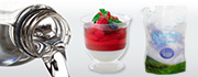 Packaging materials
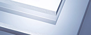
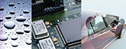 diX Coatings
- Top
- Business
- Electronics
- Semiconductor material
Semiconductor material
We deal with a wide range of material from general semiconductor materials to semiconductor devices as well as developing customized products to general-purpose products.
Customer market
General semiconductor material (semiconductor pre and post process materials, packaging materials, tools), semiconductor device
Features
- Accurate advice and planning to customers with consultation.
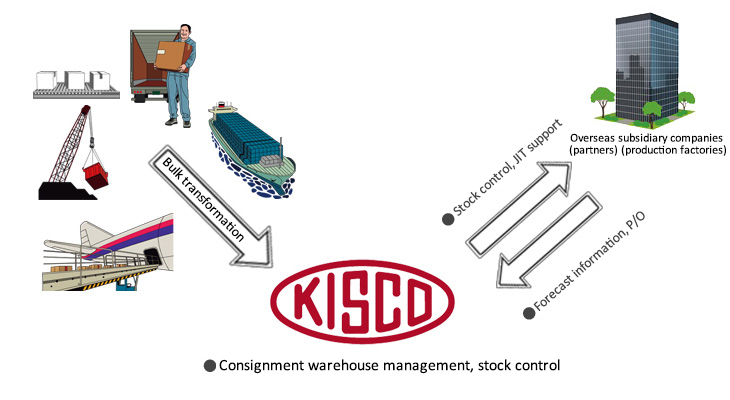
- For our customers who have exporting issues, our highly experienced staff in our subsidiary companies in China and other ASEAN countries can support you.
- Our local staff will work with you closely regarding deliveries, stock control and cash flow. We assure that you are given quality service.
KISCO’s VMI (Vendor Managed Inventory) services
Product lineup
Compound wafer, Silicone wafer, target raw material, photosensitive solvent, protection membrane material, lead frame, wire harness, boards, solder, adhesive, sealing material, ACP conductive adhesive, dicing tape, back grind tape, wafer box, chip tray, gel chip tray, carrier tape, IC tray, vacuumed process tray, desiccative wire bonding, x-ray device, ultrasound apparatus, barcode reader, tape winding device, evacuating apparatus, electrostatic countermeasure device (ESD)
Please feel free to contact us about our products.
postcode 103-8410
11-2, Nihonbashi Honcho 4-chome, Chuo-ku, Tokyo, 103-8410
3rd Sales Division Semiconductor Material Department
Tokyo Semiconductor Material Team
TEL:+81-3-3663-0276
FAX:+81-3-3661-0037
postcode 541-8513
3-7, Fushimimachi 3-chome, Chuo-ku, Osaka, 541-8513
3rd Sales Division Semiconductor Material Department
Osaka Semiconductor Material Team
TEL : +81-6-6202-2268
FAX : +81-6-6222-3027
- Business
-
- Synthetic resin
- Chemicals, food, biotechnology
- Electronics
- Packaging materials
- diX Coatings